I wanted to share my love for one of the finest pieces of open-source software around. As a long-time hardware engineer, I’ve done some PCB layout over the years with tools that included tape and a light table (I never want to do that again!), PADS PowerPCB (very capable, but difficult to use. That was years ago, so it is probably significantly different now), and Altium (reasonable price for a very capable program). However, for years I had wanted a schematic capture and PCB layout tool for personal projects, but didn’t find one that I liked or could afford. I didn’t like EAGLE’s schematic capture and then after they were acquired by AutoDesk, the pricing was more than I wanted to pay for infrequent use *. I tried using gEDA and instantly had a headache and needed to lie down.
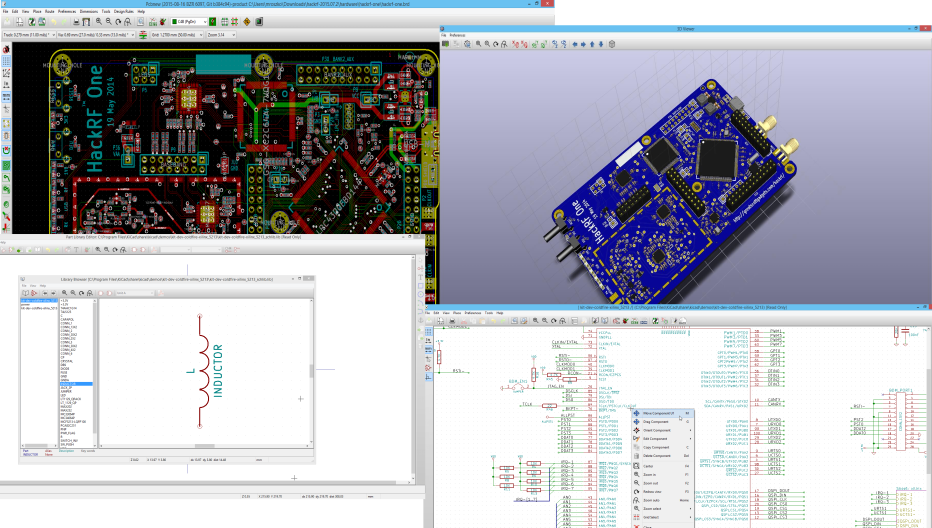
I tried an earlier version of KiCad, but was not impressed. However, in recent years, after hearing more buzz about KiCad, I tried it again and was blown away! It was now a cohesive set of tools with a fairly straightforward workflow. I was able to pick it up and learn enough to knock out a simple schematic and PCB in a day or so. When you combine these tools with low-cost PCB fab **, it is empowering for makers everywhere!
By the way, it’s pronounced “KeeCad”. I won’t ostracize you for pronouncing it other ways, but I may shoot you a look of exasperation or possibly annoyance.
As of the time of this post I’m using KiCad v5.1.8 and, although it’s not perfect, I still think it’s a shining example of what open-source development can accomplish.
g.k
* I wish I could say that I foresaw the problems with AutoDesk taking over EAGLE, but mainly I didn’t like their UI from an aesthetic and usability standpoint. I had already started using KiCad by the time the dreaded EAGLE subscription model started.
** Professional PCB fabrication used to be something that was out of the question for the DIY market. I’ve made some PCBs at home, but the lack of soldermask and silkscreen always made it look like something I wanted to hide away inside a box. I’ll have to write about PCB fab in another post.